Microchips
Overview
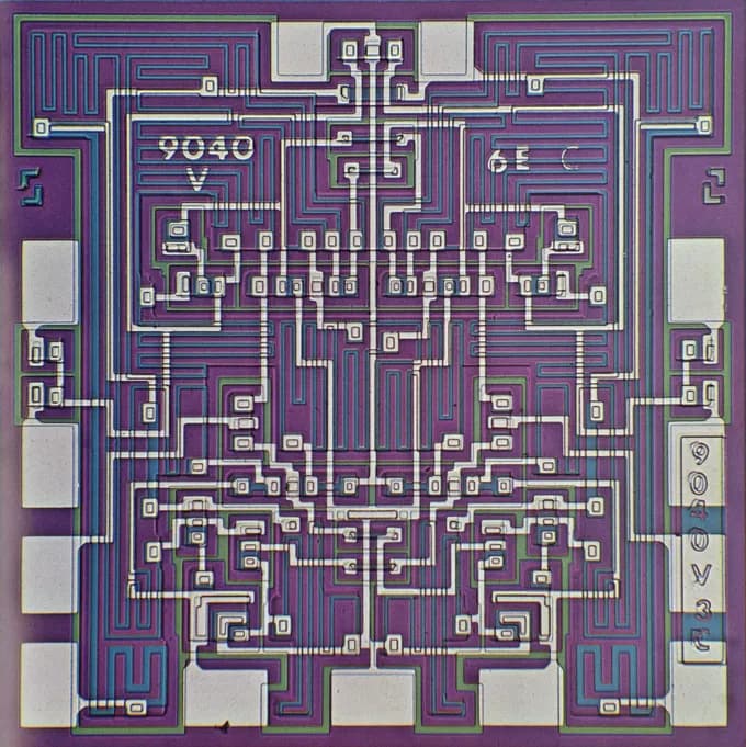
Microchips are examples of integrated circuits—chips of semiconducting material whose surfaces contain billions of circuit components wired together.
ICs were invented to solve the "tyranny of numbers," where computers had become so large that their maintenance offset computational gains. With the invention of transistors—microscopic on-off switches made of material that could conduct or insulate against the flow of electricity—the processing of binary code could be miniaturized.
Today, rather than manually assembling transistors and other circuit components onto silicon chips, fabrication labs automate manufacturing thanks largely to photolithography. Light is shone on different parts of silicon wafers, making them sensitive to various chemicals that can be applied in dozens of layers to build up circuit components and their connections.
Their ability to be reliably mass-produced and transmit electrical signals with minimal energy loss and delay has made ICs the backbone of all modern electronics.
1440 Findings
Hours of research by our editors, distilled into minutes of clarity.
Explore Science & Technology
Dive into the dynamic world of science and technology, where curiosity has brought about extraordinary understandings of the universe and creativity has led to the breakthroughs and innovations that have transformed our world. Explore a wide range of topics, from the natural and physical sciences to cutting-edge technologies and the people who shaped them, each of which is accompanied by carefully curated resources meant to inform, engage, and inspire those eager to uncover the nature of reality.
Featured Topics
- 3D Printing
- Algae
- Algorithms
- Asteroids
- Atoms
- Auroras
- Batteries
- Big Bang
- Bill Nye
- Biological Cells
- Bioluminescence
- Bioremediation
- Biosphere 2
- Black Holes
- Chaos Theory
- Climatology
- Comets
- Computer Viruses
- Coral Reefs
- Critical Minerals
- Crude Oil
- Cryptography
- Dark Energy
- Dark Matter
- Dark Web
- Data Centers
- David Attenborough
- Deep-Sea Mining
- Deepfakes
- Dinosaurs
- DNA
- Earth
- Earth's Atmosphere
- Earthquakes
- El Niño-Southern Oscillation
- Electric Grids
- Electric Vehicles
- Electricity
- Environmental Protection Agency
- Extremophiles
- Fireworks
- Fracking
- General Relativity
- Generative AI
- Geothermal Power
- Grace Hopper
- Graphics Processing Unit
- Greenhouse Gases
- Helium
- Hubble Space Telescope
- Hurricanes
- International Space Station
- Internet
- Invasive Species
- James Webb Space Telescope
- Jupiter
- Large Hadron Collider
- Large Language Models
- Lasers
- Light
- Lightning
- LIGO
- Marie Curie
- Mars
- Memory
- Microchips
- Microplastics
- Mixed Reality
- Molecular Gastronomy
- NASA
- National Science Foundation
- Neutron Stars
- Nikola Tesla
- Nobel Prize
- Nuclear Power
- Particle Accelerators
- Photosynthesis
- Plate Tectonics
- Pollinators
- Pontifical Academy of Sciences
- Quantum Computing
- Quantum Mechanics
- Radioactivity
- Rosalind Franklin
- Scientific Theory
- Self-Driving Cars
- Smart Cities
- Solar Power
- Sound
- Space Shuttle
- Space Tourism
- Space Trash
- Standard Model
- Stephen Hawking
- Sun
- Tardigrades
- Tesla
- Time
- Tornadoes
- Turbulence
- Viking Project
- Volcanoes
- Voyager Mission
- Water
- Wikipedia
- Wind Power